








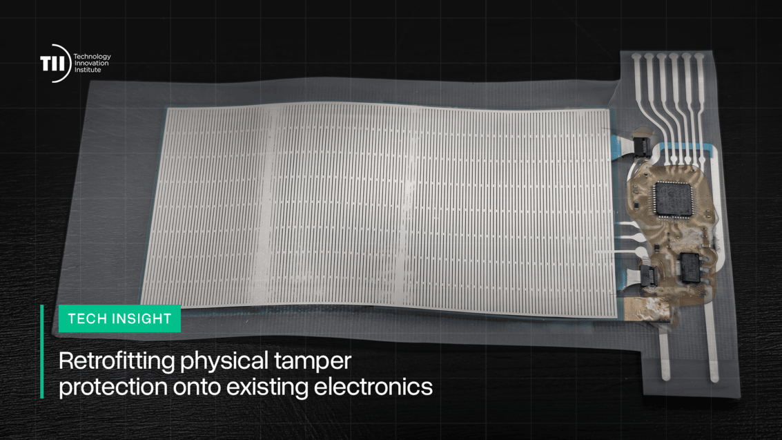
Research at the Secure Systems Research Center has developed a printed detection layer that can be applied to a circuit board after it has been designed.
In considering device security, the assumed causes for concern are encryption, secure boot, and confidentiality. But buyers of security-sensitive electronics increasingly require proof that a product resists physical attack, evidence that an adversary in possession of the device, with a workbench, some tools, and time, cannot extract what is held inside it. In regulated sectors, that proof is now a procurement condition rather than an engineering preference.
The industry meets this at chip level on day one: anti-tamper is built into the silicon with protection specified in the opening weeks of a design cycle and fixed from that point on. Wire mesh enclosures, piezoelectric sheets and fiber-optic loops are engineered around a specific printed circuit board, which means the layout has to be known before the protection can be built. Nothing retrofits and hardware that is already designed and in the field cannot be upgraded. If extra assurance is needed, this leads to two options: redesign the silicon or ship the exposure.
Research at the Technology Innovation Institute’s Secure Systems Research Center has developed a third option: a protective layer applied over an existing board called AEGARD Shield.
This layer makes physical access harder, detects drilling, cutting, bending, and probing as they happen, leaves evidence of an attack after the fact, and signals the host so that lockdown or key deletion can be triggered.
The research team did not set out to invent new inks or new functional materials. Their layer works with established printing processes and commercially available materials since even the best shield is worth little if it cannot be manufactured at volume.
AEGARD Shield is a hybrid of a printed wire-mesh sensor which registers solvent exposure, mechanical probing and drilling at sub-millimeter scale, and a piezoelectric sensor that generates an electric charge when it experiences mechanical stress or pressure. The result is a thin polyurethane film carrying a stretchable detection mesh and its circuitry, screen printed and then laminated onto the target hardware. Screen printing is fast and has a credible path to automation and the lamination method attaches the sensor without a separate adhesive layer, which minimizes the mass and thickness added to the host device.
A retrofitted shield will not match a protection scheme designed into the silicon from the start, but AEGARD is not intended to. It is an additional layer of protection.
The research team has two problems to solve still. The first is environmental durability: a printed sensor bonded to a board has to survive the temperature and humidity range specified for the product it protects. The second is discrimination: a layer sensitive enough to register a probe tip also registers the ordinary mechanical life of the device it sits on, and separating intrusion from beign vibration remains a classification problem.
Both problems are the work that turns a proof of concept into a product but with this development so far, protection can now be introduced at any stage of a product’s life cycle. Almost everything in this field has been built for new hardware and the installed base has been left out of the conversation. The device an adversary can physically reach is rarely the one still on the drawing board. AEGARD Shield exists to protect those devices already in the field.